Examples
Defect engineering in a Crystal Lattice
Klein et al., Nature, 2026 MIT · National Laboratory of the Rockies · Oak Ridge National Laboratory · Radboud University · King’s College London
In this paper we report the first demonstration of deterministic, large-scale atomic engineering inside a 3D crystal, moving well beyond the first work demonstrating atom manipulation on a crystal surface, pioneered by Eigler and Schweizer in 1990. Using a focused electron beam in a scanning transmission electron microscope (STEM), the authors precisely steer individual chromium Cr atoms within the layered magnetic semiconductor CrSBr into selected interstitial positions, creating user-defined vacancy–interstitial defect pairs throughout a 3D volume. In so doing they created a periodically ordered “artificial crystal” composed of more than 40,000 user-defined defects within about 40 minutes, across a 150 nm × 100 nm × 13 nm volume.
Unlike previous atomic manipulation techniques that were restricted to surfaces (such as STM tip manipulation) or lacked scalability, this approach allows for the creation of stable, sub-surface defect arrays with programmable spacings and tunable quantum interactions.
Experimental Details
- A 200 keV electron beam is positioned onto target Cr atomic columns. To manipulate the atoms without destroying the lattice, the team developed beam-control algorithms capable of positioning the electron beam with sub-20-pm-scale accuracy.
- The beam executes programmed oscillatory motions (e.g., back-and-forth along crystal axes), knocking Cr atoms into adjacent interstitial sites.
- Directional displacement: By driving the electron beam along specific vertical, horizontal, or diagonal paths (e.g. rotating the beam trajectory by 90°) they selectively steered chromium Cr atoms into different neighboring interstitial sites, generating distinct types of vacancy-interstitial complexes (e.g., and ). Ten unique defect configurations were demonstrated.
- Electron channeling: through the crystal lattice guides the beam consistently through the full thickness — not just the surface layer. After one Cr atom is displaced, adjacent atoms in layers above/below shift in the opposite direction via a cascading displacement mechanism, propagating the defect column through the bulk.
- Ambient stability: The engineered artificial defect lattices remain structurally stable at room temperature and outside the microscope, making them viable for external applications.
Mechanism
Density functional theory (DFT) calculations revealed that Cr displacement occurs through a bond-switching mechanism. When moving from a lattice site to an interstitial site, the Cr atom preserves one of its original four Cr-S bonds while replacing the other three with Cr-Br bonds. This minimal disruption facilitates smooth, reversible migration. This directional control is highly rate-dependent and works optimally at high beam energies (200 keV), where inelastic electron excitation transiently lowers migration barriers while elastic momentum transfer provides a directional push. At lower energies (100 keV), directional selectivity is lost due to localized material damage overtaking the slow migration rate.
Theory
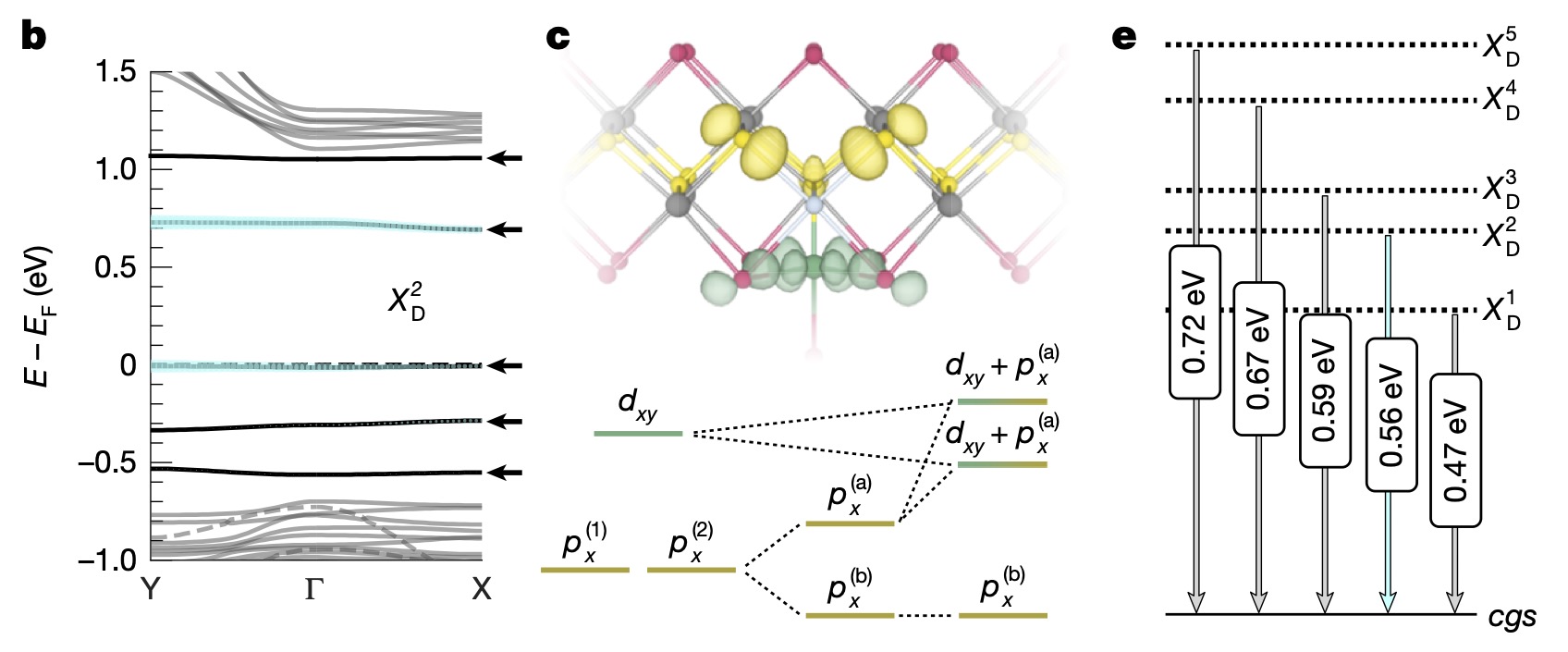 Fig. 1. b, QSGŴ electronic band structure of with host bands (grey) and five defect bands (black). The -space contribution of one of the five excitonic bound states () is highlighted (). c, Orbital and electronic level structure of . e, Bound exciton-level diagram from BSE calculations. For a description of QSGŴ theory, see this paper.
First-principles calculations using Quasiparticle Self-Consistent GW (QSGW) theory indicate that the primary defect, the isolated complex, behaves as a strongly correlated quantum object, carrying electronic structures reminiscent of NV centers in diamond. Theory shows that the defect introduces five flat mid-gap impurity states. The partial occupation of these states leads to tightly bound intra-defect excitons, with excitonic resonances appearing in the near- to mid-infrared spectrum.
When arranged into arrays, the long-ranged () inter-defect Coulomb interactions yield highly tunable coupling strengths. Because out-of-plane electron hopping is suppressed in the material’s antiferromagnetic phase, the defect arrays can effectively simulate strongly correlated 2D physics operating deep in the strong-coupling regime.
The defect superlattice forms a mesoscale crystal embedded within the host crystal — a new form of artificial matter confirmed by sharp superlattice Bragg reflections in electron diffraction.
Outlook
This methodology establishes a generalizable platform for solid-state atomic manufacturing, beyond CrSBr:
- Scalable Quantum Technologies: deterministic placement of color centers spin-photon interfaces (e.g., NV centers), scaling to millions of ordered defects within a day, for quantum networks and sensing
- Quantum simulation: programmable many-body Hamiltonians with tunable Coulomb interactions, inaccessible to cold-atom or Moiré systems.
PAPERS · DEFECT ENGINEERING · OPTICAL RESPONSE · MANY BODY PERTURBATION THEORY